- 您现在的位置:买卖IC网 > Sheet目录494 > NVTFS5820NLTAG (ON Semiconductor)MOSFET N-CH 60V 37A 8WDFN
�� �
�
�NVTFS5820NL�
�Power� MOSFET�
�60� V,� 11.5� m� W� ,� Single� N� ?� Channel,� m� 8FL�
�Features�
�?� Small� Footprint� (3.3x3.3� mm)� for� Compact� Design�
�?� Low� R� DS(on)� to� Minimize� Conduction� Losses�
�?� Low� Q� G� and� Capacitance� to� Minimize� Driver� Losses�
�?� NVTFS5820NLWF� ?� Wettable� Flanks� Product�
�?� AEC� ?� Q101� Qualified� and� PPAP� Capable�
�?� These� Devices� are� Pb� ?� Free� and� are� RoHS� Compliant�
�MAXIMUM� RATINGS� (T� J� =� 25� °� C� unless� otherwise� noted)�
�V� (BR)DSS�
�60� V�
�http://onsemi.com�
�R� DS(on)� MAX�
�11.5� m� W� @� 10� V�
�15� m� W� @� 4.5� V�
�I� D� MAX�
�29� A�
�Parameter�
�Drain� ?� to� ?� Source� Voltage�
�Gate� ?� to� ?� Source� Voltage�
�Symbol�
�V� DSS�
�V� GS�
�Value�
�60�
�"� 20�
�Unit�
�V�
�V�
�N� ?� Channel�
�D�
�Continuous� Drain� Cur-�
�rent� R� Y� J� ?� mb� (Notes� 1,�
�2,� 3,� 4)�
�Power� Dissipation�
�R� Y� J� ?� mb� (Notes� 1,� 2,� 3)�
�Steady�
�State�
�T� mb� =� 25� °� C�
�T� mb� =� 100� °� C�
�T� mb� =� 25� °� C�
�T� mb� =� 100� °� C�
�I� D�
�P� D�
�29�
�20�
�21�
�10�
�A�
�W�
�G�
�S�
�T� A� =� 25� °� C�
�Continuous� Drain� Cur-�
�rent� R� q� JA� (Notes� 1� &�
�3,� 4)�
�Power� Dissipation�
�R� q� JA� (Notes� 1,� 3)�
�Pulsed� Drain� Current�
�T� A� =� 25� °� C�
�Steady� T� A� =� 100� °� C�
�State�
�T� A� =� 100� °� C�
�T� A� =� 25� °� C,� t� p� =� 10� m� s�
�I� D�
�P� D�
�I� DM�
�11�
�8.0�
�3.2�
�1.6�
�247�
�A�
�W�
�A�
�1�
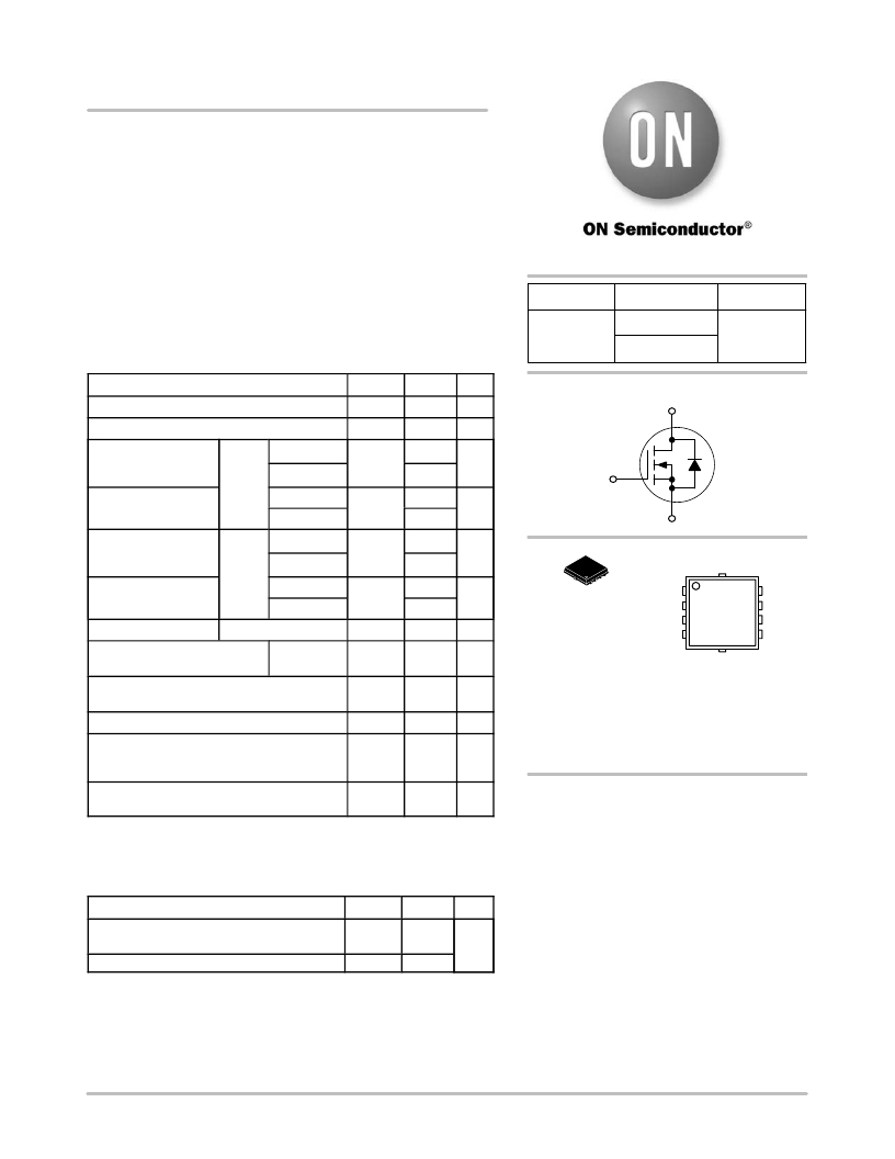
�WDFN8�
�(� m� 8FL)�
�CASE� 511AB�
�MARKING� DIAGRAM�
�1�
�S� D�
�S� XXXX� D�
�S� AYWW� G� D�
�G� G� D�
�Current� limited� by� package� T� A� =� 25� °� C�
�(Note� 4)�
�Operating� Junction� and� Storage� Temperature�
�I� DmaxPkg�
�T� J� ,� T� stg�
�70�
�?� 55� to�
�175�
�A�
�°� C�
�XXXX�
�A�
�Y�
�=� Specific� Device� Code�
�=� Assembly� Location�
�=� Year�
�Source� Current� (Body� Diode)�
�Single� Pulse� Drain� ?� to� ?� Source� Avalanche�
�Energy� (T� J� =� 25� °� C,� V� DD� =� 50� V,� V� GS� =� 10� V,�
�I� L(pk)� =� 31� A,� L� =� 0.1� mH,� R� G� =� 25� W� )�
�Lead� Temperature� for� Soldering� Purposes�
�(1/8� ″� from� case� for� 10� s)�
�I� S�
�E� AS�
�T� L�
�17�
�48�
�260�
�A�
�mJ�
�°� C�
�WW� =� Work� Week�
�G� =� Pb� ?� Free� Package�
�(Note:� Microdot� may� be� in� either� location)�
�ORDERING� INFORMATION�
�Stresses� exceeding� Maximum� Ratings� may� damage� the� device.� Maximum�
�Ratings� are� stress� ratings� only.� Functional� operation� above� the� Recommended�
�Operating� Conditions� is� not� implied.� Extended� exposure� to� stresses� above� the�
�Recommended� Operating� Conditions� may� affect� device� reliability.�
�THERMAL� RESISTANCE� MAXIMUM� RATINGS� (Note� 1)�
�See� detailed� ordering,� marking� and� shipping� information� in� the�
�package� dimensions� section� on� page� 5� of� this� data� sheet.�
�Parameter�
�Junction� ?� to� ?� Mounting� Board� (top)� ?� Steady�
�State� (Note� 2,� 3)�
�Junction� ?� to� ?� Ambient� ?� Steady� State� (Note� 3)�
�Symbol�
�R� Y� J� ?� mb�
�R� q� JA�
�Value�
�7.3�
�47�
�Unit�
�°� C/W�
�1.� The� entire� application� environment� impacts� the� thermal� resistance� values� shown,�
�they� are� not� constants� and� are� only� valid� for� the� particular� conditions� noted.�
�2.� Psi� (� Y� )� is� used� as� required� per� JESD51� ?� 12� for� packages� in� which�
�substantially� less� than� 100%� of� the� heat� flows� to� single� case� surface.�
�3.� Surface� ?� mounted� on� FR4� board� using� a� 650� mm� 2� ,� 2� oz.� Cu� pad.�
�4.� Maximum� current� for� pulses� as� long� as� 1� second� is� higher� but� is� dependent�
�on� pulse� duration� and� duty� cycle.�
�?� Semiconductor� Components� Industries,� LLC,� 2013�
�September,� 2013� ?� Rev.� 4�
�1�
�Publication� Order� Number:�
�NVTFS5820NL/D�
�发布紧急采购,3分钟左右您将得到回复。
相关PDF资料
NVTFS5826NLTAG
MOSFET N-CH 60V 20A 8WDFN
NX201103
SYNJET ZFLOW 87 LEVEL SELECT 12V
NX300106
HEATSINK 43W TWIST GE INFUSION
NX300119
HEATSINK 70W SPOT CONFIG
NX300131
HEATSINK 58W TWIST MODULE COOLER
NX300146
HEATSINK 82W WALLWASHER RECT
OD-100
EMITTER IR 100MW 880NM TO-39
OD-110L
IR EMITTER 110MW 850NM
相关代理商/技术参数
NVTFS5820NLTWG
功能描述:MOSFET Single N-Channel 60V,29A,11.5mohm RoHS:否 制造商:STMicroelectronics 晶体管极性:N-Channel 汲极/源极击穿电压:650 V 闸/源击穿电压:25 V 漏极连续电流:130 A 电阻汲极/源极 RDS(导通):0.014 Ohms 配置:Single 最大工作温度: 安装风格:Through Hole 封装 / 箱体:Max247 封装:Tube
NVTFS5826NL
制造商:ONSEMI 制造商全称:ON Semiconductor 功能描述:150 mA, Ultra Low Supply Current, Low Dropout Regulator
NVTFS5826NLTAG
功能描述:MOSFET Single N-Channel 60V,20A,24mohm
RoHS:否 制造商:STMicroelectronics 晶体管极性:N-Channel 汲极/源极击穿电压:650 V 闸/源击穿电压:25 V 漏极连续电流:130 A 电阻汲极/源极 RDS(导通):0.014 Ohms 配置:Single 最大工作温度: 安装风格:Through Hole 封装 / 箱体:Max247 封装:Tube
NVTFS5826NLTWG
功能描述:MOSFET Single N-Channel 60V,20A,24mohm RoHS:否 制造商:STMicroelectronics 晶体管极性:N-Channel 汲极/源极击穿电压:650 V 闸/源击穿电压:25 V 漏极连续电流:130 A 电阻汲极/源极 RDS(导通):0.014 Ohms 配置:Single 最大工作温度: 安装风格:Through Hole 封装 / 箱体:Max247 封装:Tube
NVTFS5826NLWFTAG
制造商:ONSEMI 制造商全称:ON Semiconductor 功能描述:60 V, 24 m, 20 A, Single Na??Channel
NVTFS5826NLWFTWG
制造商:ONSEMI 制造商全称:ON Semiconductor 功能描述:60 V, 24 m, 20 A, Single Na??Channel
NVTGS3455T1G
功能描述:MOSFET N-CH 30V 3.5A 6-TSOP RoHS:是 类别:分离式半导体产品 >> FET - 单 系列:* 标准包装:1,000 系列:MESH OVERLAY™ FET 型:MOSFET N 通道,金属氧化物 FET 特点:逻辑电平门 漏极至源极电压(Vdss):200V 电流 - 连续漏极(Id) @ 25° C:18A 开态Rds(最大)@ Id, Vgs @ 25° C:180 毫欧 @ 9A,10V Id 时的 Vgs(th)(最大):4V @ 250µA 闸电荷(Qg) @ Vgs:72nC @ 10V 输入电容 (Ciss) @ Vds:1560pF @ 25V 功率 - 最大:40W 安装类型:通孔 封装/外壳:TO-220-3 整包 供应商设备封装:TO-220FP 包装:管件
NVTJD4001NT1G
功能描述:MOSFET NFET 30V 250MA 1.5OH RoHS:否 制造商:STMicroelectronics 晶体管极性:N-Channel 汲极/源极击穿电压:650 V 闸/源击穿电压:25 V 漏极连续电流:130 A 电阻汲极/源极 RDS(导通):0.014 Ohms 配置:Single 最大工作温度: 安装风格:Through Hole 封装 / 箱体:Max247 封装:Tube